- 您现在的位置:买卖IC网 > Sheet目录1997 > ICS843021AGLFT (IDT, Integrated Device Technology Inc)IC CLK GENERATOR LVPECL 8-TSSOP
ICS843021AG REVISION D OCTOBER 12, 2010
9
2010 Integrated Device Technology, Inc.
ICS843021 Data Sheet
FEMTOCLOCK CRYSTAL-TO-3.3V LVPECL CLOCK GENERATOR
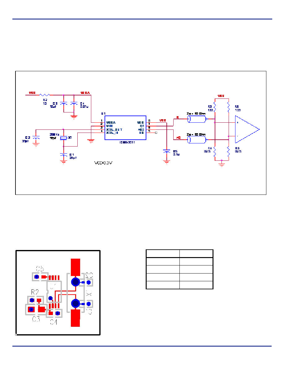
Schematic Example
Figure 5A shows a schematic example of using an ICS843021. An
example of LVPECL termination is shown in this schematic.
Additional LVPECL termination approaches are shown in the
LVPECL Termination Application Note. In this example, an 18pF
parallel resonant crystal is used for generating 125MHz output
frequency. TheC1 = 27pF and C2 = 33pF are recommended for
frequency accuracy. For a different board layout, the C1 and C2
values may be slightly adjusted for optimizing frequency accuracy.
Figure 5. ICS843021 Schematic Example
Schematic Example
Figure 5B shows an example of ICS843021 P.C. board layout. The
crystal X1 footprint shown in this example allows installation of either
surface mount HC49S or through-hole HC49 package. The footprints
of other components in this example are listed in the Table 7 There
should be at least one decoupling capacitor per power pin. The
decoupling capacitors should be located as close as possible to the
power pins. The layout assumes that the board has clean analog
power ground plane.
Figure 5B. ICS843021 PC Board Layout Example
Table 7. Footprint Table
NOTE: Table 7 lists component sizes
shown in this layout example.
Reference
Size
C1, C2
0402
C3
0805
C4, C5
0603
R2
0603
发布紧急采购,3分钟左右您将得到回复。
相关PDF资料
ICS843022AGLF
IC CLK GENERATOR LVPECL 8-TSSOP
ICS843023AGLF
IC CLK GENERATOR LVPECL 8-TSSOP
ICS843031AG-01LF
IC CLK GENERATOR LVPECL 8-TSSOP
ICS843081AGI-01LF
IC CLK MULTIPLIER LVPECL 8-TSSOP
ICS8430AYI-61LF
IC SYNTHESIZER LVPECL 32-LQFP
ICS8430S07AKILF
IC CLK GENERATOR PLL 32VFQFN
ICS8430S10BYI-02LF
IC CLK GENERATOR PLL 48TQFP
ICS84314AY-02LFT
IC SYNTHESIZER 700MHZ 32-LQFP
相关代理商/技术参数
ICS843021AGT
制造商:ICS 制造商全称:ICS 功能描述:FEMTOCLOCKS-TM CRYSTAL-TO- 3.3V LVPECL CLOCK GENERATOR
ICS843021I-01
制造商:ICS 制造商全称:ICS 功能描述:FEMTOCLOCKS-TM CRYSTAL-TO-3.3V, 2.5V 125MHZ LVPECL CLOCK GENERATOR
ICS843022
制造商:ICS 制造商全称:ICS 功能描述:FEMTOCLOCKS-TM CRYSTAL-TO- 3.3V LVPECL CLOCK GENERATOR
ICS843022AG
制造商:INT_DEV_TECH 功能描述:
ICS843022AGI-48LF
功能描述:IC CLK SYNTHESIZER LVPECL 8TSSOP RoHS:是 类别:集成电路 (IC) >> 时钟/计时 - 时钟发生器,PLL,频率合成器 系列:HiPerClockS™, FemtoClock™ 标准包装:1,000 系列:- 类型:时钟/频率合成器,扇出分配 PLL:- 输入:- 输出:- 电路数:- 比率 - 输入:输出:- 差分 - 输入:输出:- 频率 - 最大:- 除法器/乘法器:- 电源电压:- 工作温度:- 安装类型:表面贴装 封装/外壳:56-VFQFN 裸露焊盘 供应商设备封装:56-VFQFP-EP(8x8) 包装:带卷 (TR) 其它名称:844S012AKI-01LFT
ICS843022AGI-48LFT
功能描述:IC CLK SYNTHESIZER LVPECL 8TSSOP RoHS:是 类别:集成电路 (IC) >> 时钟/计时 - 时钟发生器,PLL,频率合成器 系列:HiPerClockS™, FemtoClock™ 标准包装:1,000 系列:- 类型:时钟/频率合成器,扇出分配 PLL:- 输入:- 输出:- 电路数:- 比率 - 输入:输出:- 差分 - 输入:输出:- 频率 - 最大:- 除法器/乘法器:- 电源电压:- 工作温度:- 安装类型:表面贴装 封装/外壳:56-VFQFN 裸露焊盘 供应商设备封装:56-VFQFP-EP(8x8) 包装:带卷 (TR) 其它名称:844S012AKI-01LFT
ICS843022AGLF
功能描述:IC CLK GENERATOR LVPECL 8-TSSOP RoHS:是 类别:集成电路 (IC) >> 时钟/计时 - 时钟发生器,PLL,频率合成器 系列:HiPerClockS™, FemtoClock™ 标准包装:1,000 系列:- 类型:时钟/频率合成器,扇出分配 PLL:- 输入:- 输出:- 电路数:- 比率 - 输入:输出:- 差分 - 输入:输出:- 频率 - 最大:- 除法器/乘法器:- 电源电压:- 工作温度:- 安装类型:表面贴装 封装/外壳:56-VFQFN 裸露焊盘 供应商设备封装:56-VFQFP-EP(8x8) 包装:带卷 (TR) 其它名称:844S012AKI-01LFT
ICS843022AGLFT
功能描述:IC CLK GENERATOR LVPECL 8-TSSOP RoHS:是 类别:集成电路 (IC) >> 时钟/计时 - 时钟发生器,PLL,频率合成器 系列:HiPerClockS™, FemtoClock™ 标准包装:1,000 系列:- 类型:时钟/频率合成器,扇出分配 PLL:- 输入:- 输出:- 电路数:- 比率 - 输入:输出:- 差分 - 输入:输出:- 频率 - 最大:- 除法器/乘法器:- 电源电压:- 工作温度:- 安装类型:表面贴装 封装/外壳:56-VFQFN 裸露焊盘 供应商设备封装:56-VFQFP-EP(8x8) 包装:带卷 (TR) 其它名称:844S012AKI-01LFT